
| Home | Probes | Applications | About us | Contacts | ||
Diamond |
SCD probes for AFM are monocrystal diamond tips grown in chemical vapor deposition process (CVD) and attached to silicon etched cantilevers. The SCD probes obtained by this method are durable and chemically inert, providing similar tip radius and much higher aspect ratio in comparison with that of silicon tips. SCD tips are remarkable for their long life in contact or dynamic AFM regimes. The tip is quite robust and forgiving operation mistakes, while it is sharp enough to provide high resolution on DNA or lamellar structures easily. There are some results exhibiting performance of SCD probes below. |
|||
 |
 |
 |
AFM topography of rubber Teflon sample images made using SCD probe tips (click to enlarge). Courtesy of Sergei Magonov. Agilent Technologies (2008). | |
| Scan size 2x2 µm, height 50 nm | Scan size 625x625 nm, height 20 nm | Scan size 400x400 nm, height 10 nm | ||
 |
|
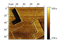
AFM topography and amplitude error images of GaN surface with hexagonal pits made using SCD probe. The pits have sharp top and bottom edges in the images, click to enlarge and see cross-sections. Scan size 5x5 µm. Courtesy of Sergei Magonov. Agilent Technologies (2008). | ||
| Topography image. Scan height 0.7 µm. | Amplitude error image. | |||
 |
 |
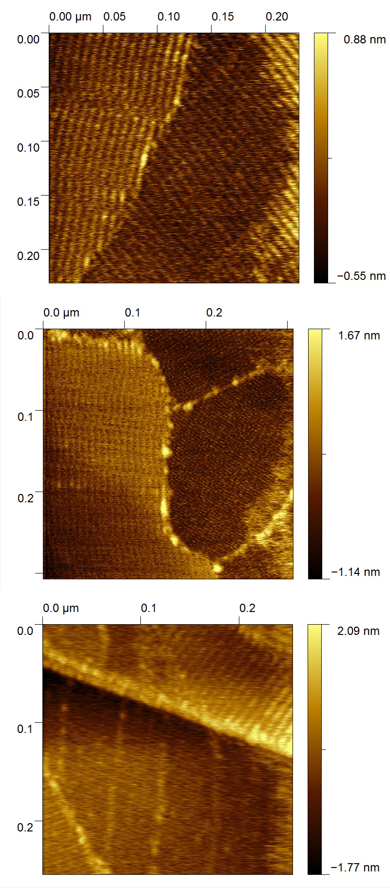
AFM topography images of a triblock copolymer film made using SCD probe (click to enlarge). Courtesy of Sergei Magonov. Agilent Technologies (2008). The scan height of 5nm is comparable to the width of some blocks, which proves the good shape of SCD tip at the end. | ||
| Scan size 2 µm, height 5nm. | Scan size 250 nm, height 5 nm. | |||
 |
 |
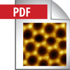
AFM topography images of C60H122 alkane layer on graphite made using SCD probe (click to enlarge). Courtesy of Sergei Magonov, Agilent Technologies (2008). | ||
| Scan size 1 µm, height 25 nm. | Scan size 250 nm, height 0.5 nm. | |||
 |
Tapping mode AFM image of a dimer molecule trapped between two electrodes made using SCD probe. Scan size 700x300 nm. Image courtesy of Sidney Cohen. Click on the image to see the cross-section of the dimer. |
|||
|
• For long scanning, when tip replacement is hard, time-taking or not compatible with the experiment;
It was also reported that SCD was used for long-time scanning of biological samples without tip contamination, which is probably related to the low surface energy of diamond. |
||||
Long Scanning, |
In spite of the sharpness and high aspect ratio, SCD tips are durable enough to provide long scanning time. This can be used for imaging processes, when the tip shape has to remain unchanged during many scans of the same surface area. SCD probes often hold the promise of not breaking even when the tip meets an obstacle on surface the feedback loop cannot process quickly. This is advantageous when the tip replacement is hard or time taking, e.g. in UHV SPM systems. Results below demonstrate the durability and wear resisnatce of SCD tips. |
|||
 |
 |
 |
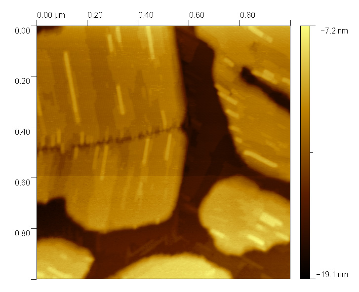
Series of experiments made by one SCD tip in the order as shown: indentation on Pt film, imaging high aspect ratio porous Al structure, imaging lamellar structure of Melissa acid. Click to enlarge.
Courtesy of Alexei Temiryazev, IRE RAS (2013). |
 |
| Scan of indents left on Pt film by SCD tip. The image is made by the same tip that made the indents. Scan size 800x800 nm, height 20 nm | Topography image of porous Aluminium structure, size 1x1 µm, height 45 nm | Lamellar structure of Melissa acid. Scan size 250x250 nm, height 1.5 nm | ||
|
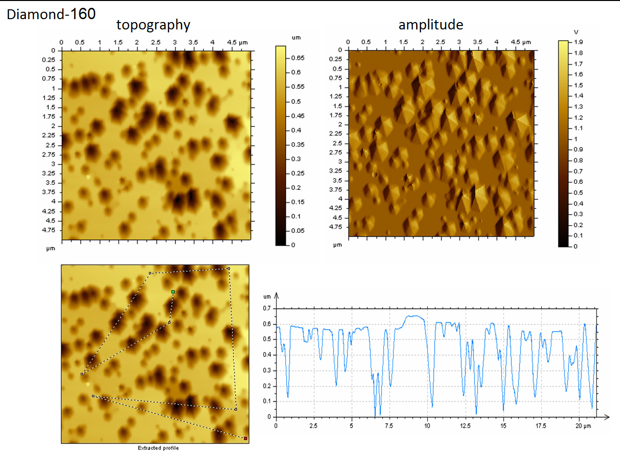
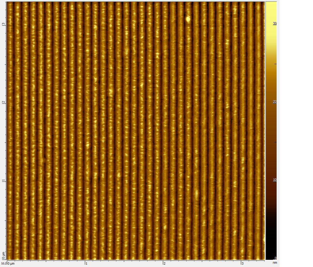
Image below is a fragment of a 121-scan each 100x100 µm mosaic made automatically on Smart-SPM in contact mode using SCD probe (click to see the full image). The sample is a magnetic test structure comprising stripes of CoCr alloy on Si surface, courtesy of Alexander Shokin, NIIFP. Each scan in the mosaic has a size of 100x100 µm, so the probe of a 5 N/m spring constant travelled 6 meters in contact mode totally to obtain the image. There is no visible wear of the SCD tip in the image. |
||||
 |
Fragment of a mosaic of 121 scan obtained automatically in Contact mode using SCD probe. CLICK to see the full image. Cantilever spring constant 5 N/m, the mosaic size is about 1x1 mm, the total path the probe made is 6 meters long.
Check application note on using SCD probe in contact mode AFM. Image courtesy of Alexei Temiryazev, AIST-NT (2010). |
 |
||
|
|
||||
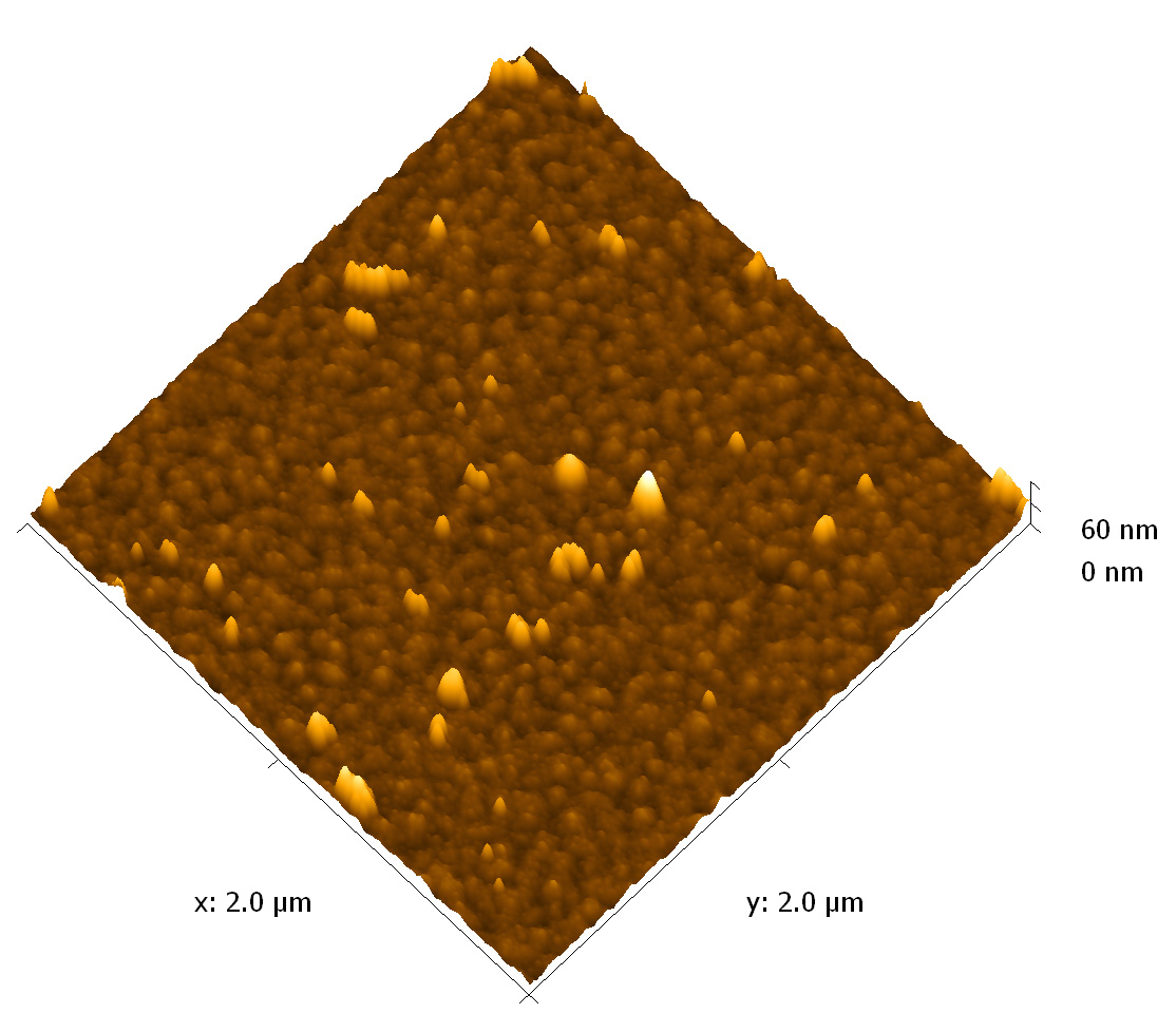 |
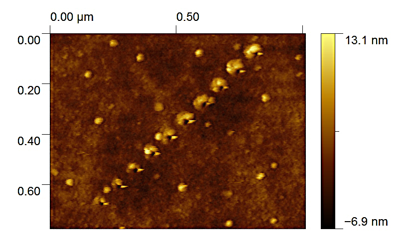
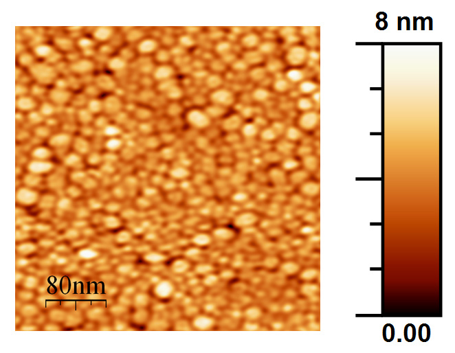
Tapping mode AFM image of gold nanoparticles bound to electrode surface made using SCD probe. Scan size 2x2 µm, height 60 nm. Image credit: Peter Eaton and Joao Cortez, Requimte, Portugal. |
|||
Scanning |
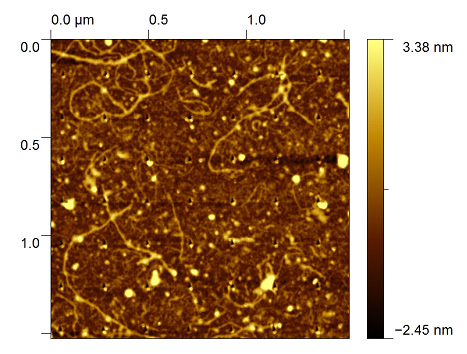
The scan of DNA made using SCD probe below shows the molecules as having a width less than 10 nm, click to see the cross-sections. Similar result is seen on collagen molecules where the feature width of collagen is about 6 nm with the diamond tip. Comparison with the regular silicon probe shows that the feature width of collagen is 30% or more lower with the diamond tip, the images are also cleaner.
|
|||
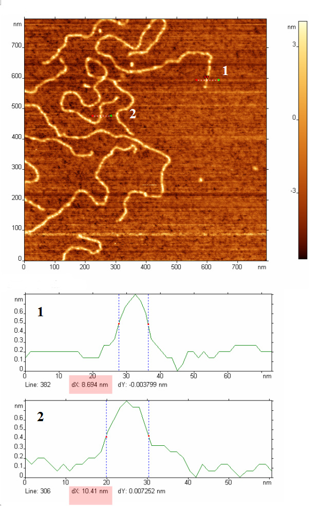 |
AFM topography of DNA made using SCD probe. Click to enlarge and see cross-sections. Image courtesy of Sergei Magonov, Agilent Technologies (2009). Scan size 800x800 nm, height 10 nm. |
|||
 |
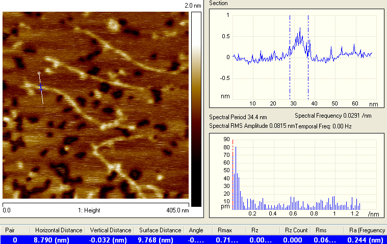 |
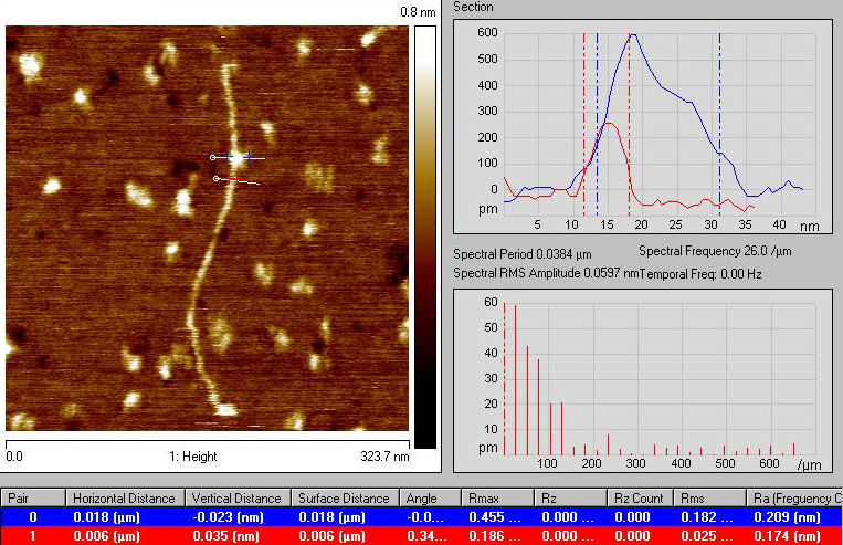
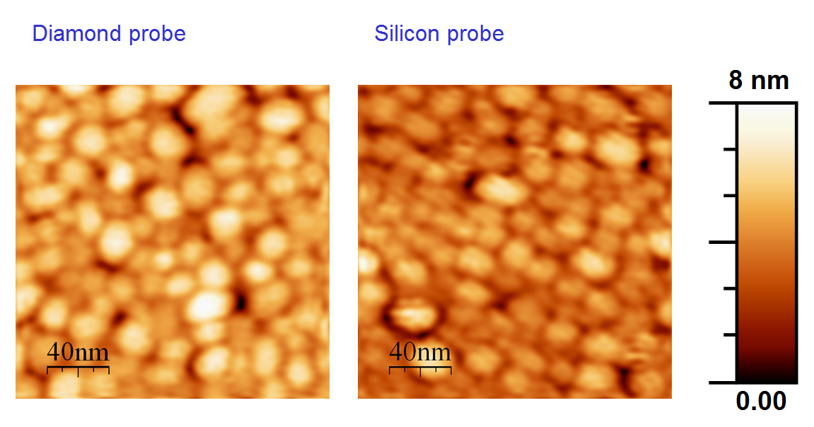
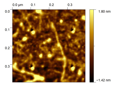
AFM topography images of a collagen molecules made using SCD (left) and Silicon (right) probes (click to enlarge and see the cross-sections). The blobs seen on the collagen are proteins attached to it, which can be seen more clearly with the diamond probe. Courtesy of Sidney Cohen.
The tip lasted for about a day of imaging. |
||
| Diamond probe. Scan size 320 nm, height 0.8 nm. |
Silicon probe. Scan size 400 nm, height 2 nm. |
|||
High |
|
|||
 |
 |
|
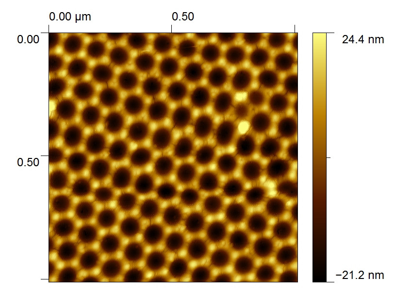
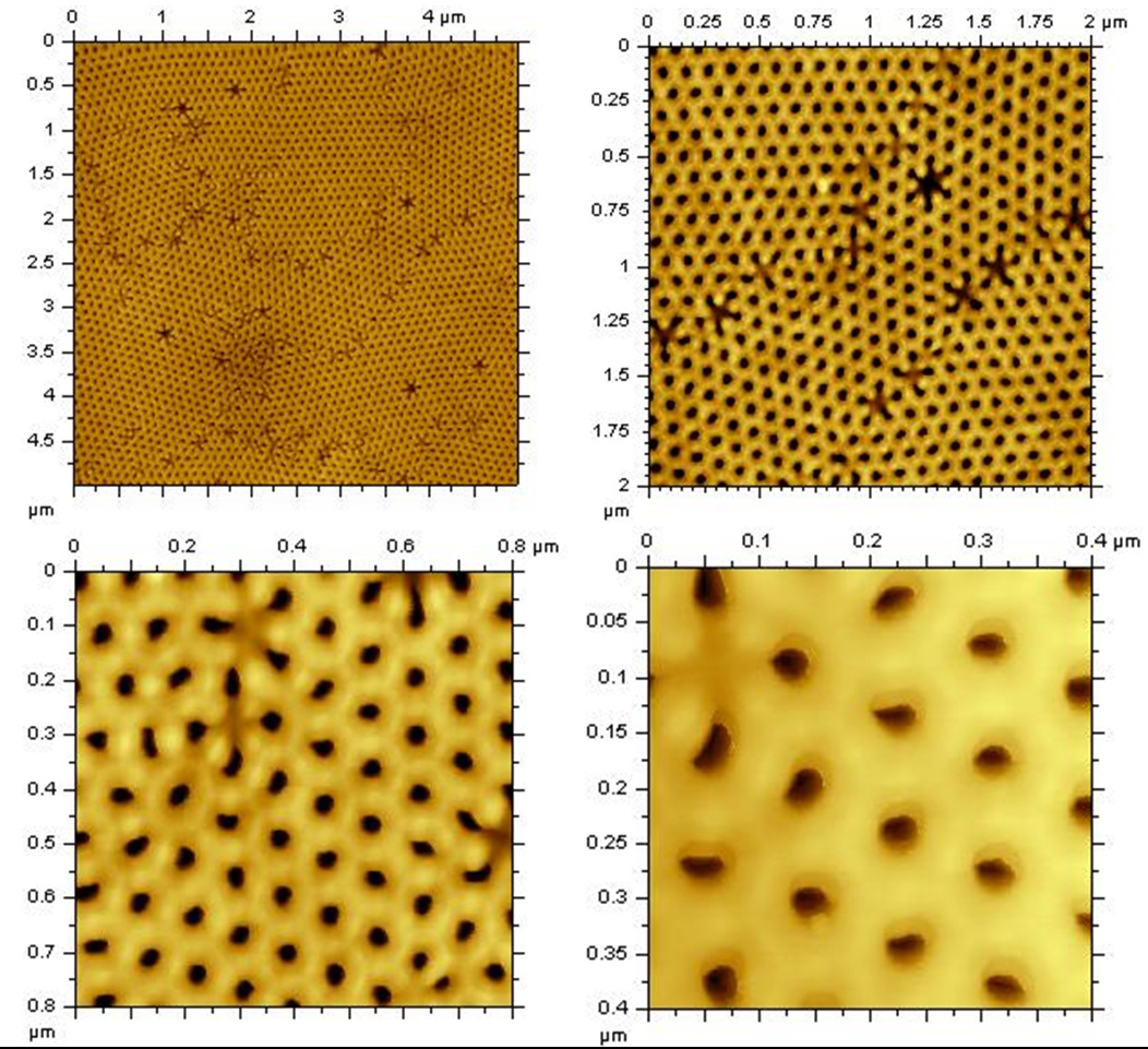
AFM topography of porous alumina made using SCD probe. Click to enlarge and see cross-sections. Courtesy of Sergei Magonov, Agilent Technologies (2008). | |
| Scan size 2 µm. | Scan sixe 800 nm. Cross-sections available, click to see. | Scan size 400 nm. | ||
|
|
||||
 |
 |
 |
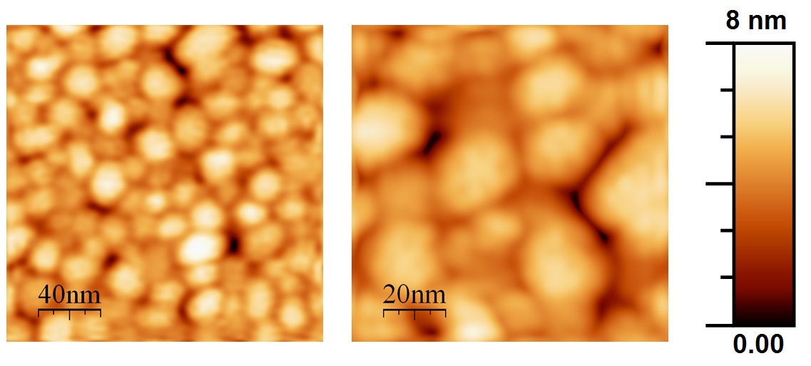
Tapping mode AFM images of gold nanoparticles made using silicon and diamond probes. Courtesy of Pavlo Mikheenko, University of Birmingham. | |
| Scan size 400 nm. Diamond probe. | Scan size 200 nm. Diamond probe. | Scan size 200 nm. Silicon probe, smaller scan height (click to compare). | ||
Materials |
|
|||
 |
 |
 |
Materials contrast image made using nanoindentation SPM by SCD probe on a semiconductor structure. Scan sizes 100x90 µm. | |
| Topography image | Loading curves | Unloading curves | ||
 |
 |
Closer views of the areas above that show the indents left by the SCD tip. The scans are made by the same tip that made the indents, the resolution is still better than 10 nm.
Courtesy of Alexei Temiryazev, IRE RAS (2013). |
 |
|
| Scan size 1.5 µm | Scan size 400 nm | |||
SPM Force |
Among other results, the paper on pulse force SPM lithography referenced below presents a grating cut on Si with the period of 30 nm and depth 5-6 nm below the zero surface level. In terms of the attainable feature sizes, FIB technique is the only alternative to SPM. FIB is widely used in industry because of its speed. Still the costs of using FIB in research and prototyping are high because of a long and complex setup procedure, while SPM lithography with diamond tips is simple and advantageous for a lab.
|
|||
 |
Grating cut on Si by SCD probe in Pulse force lithography1. The image is also made by the same SCD tip. Period 50 nm, height 6 nm.
Courtesy of Alexei Temiryazev, IRE RAS (2014). |
|||
 |
Grating cut in alloy film by scratching, material hardness about 500 GPa. Period 100 nm, depth more than 20 nm.
Courtesy of E. Huseynov, T. Mekhtiyev, Institute of Physics of ANAS. |
 |
||
1. A. Temiryazev. Pulse force nanolithography on hard surfaces using atomic force microscopy with a sharp single-crystal diamond tip. Diamond & Related Materials 48 (2014) 6064. arXiv:1312.0796 |
||||