
| Home | Probes | Applications | About us | Contacts |
|
|
Single |
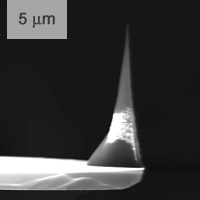
SCD probes for atomic force microscopes are single crystal diamond tips specially grown in CVD process and glued onto silicon cantilevers. The growth technology provides durable micro-sized monocrystal pyramids with high aspect ratio and small tip radius. Each tip passes quality control on SEM before mounting onto the cantilever. Beacuse of the high hardness of diamond, the tip can be used for surface modifications and measuring properties of hard materials like silicon, glass, metals, etc. The probe is highly resistant to wear, which is especially useful when fast scanning speed is needed, or when or when there are sharp and rigid edges on surface. |
||||||||||||||||
 |
 |
 |
 |
||||||||||||||
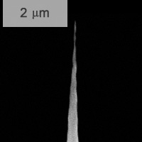
| SEM image of single crystal diamond (SCD) tip for SPM. | SEM image of the tip aspect ratio over |
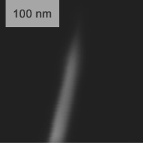
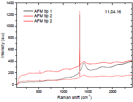
SEM image of the SCD tip end. Tip radius less than 10 nm. | Raman spectra of SCD tips. Thin diamond line at |
||||||||||||||
|
|
||||||||||||||||
Applications |
SCD diamond tip is: It was also reported that SCD probes can be used for long-time scanning of sticky biological samples without contamination, which can be related to the low surface energy of diamond >>>. |
1. A. Lipatov et al., Elastic properties of 2D Ti3C2Tx MXene monolayers and bilayers. Sci. Adv. 2018, 4, 6, eaat0491 2. A. Temiryazev. Pulse force nanolithography on hard surfaces using atomic force microscopy with a sharp single-crystal diamond tip. Diamond & Related Materials 48 (2014) 6064. arXiv:1312.0796 3. A. Krayev et al, TERS at work: 2D materials, from graphene to 2D semiconductors. Proc. SPIE 9925, Nanoimaging and Nanospectroscopy IV, 2016, 99250A 4. A. Temiryazev et al., Formation of magnetic nanostructures using an atomic force microscope probe. Tech. Phys. 2019, 64: 1716-1721. 5. R. Nelz et al, Color center fluorescence and spin manipulation in single crystal, pyramidal diamond tips. arXiv:1608.08369 6. S. Choi et al, Enhancing optical readout from diamond AFM tips for quantum nanosensing, ACS Photonics 2018, 5, 11, 4244-4248 | |
Cantilevers |
||||||||||||||||||||||
|
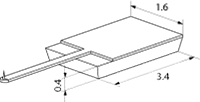
SCD diamond probes are glued onto rectangular (diving-board) silicon etched cantilevers. The range of spring constants and resonant frequencies of cantilevers available covers the Contact mode, Force Modulation, Non-Contact and Tapping mode. Cantilever backside is coated by Aluminium. The chip holder size is 1.6 mm x 3.4 mm x 0.4 mm. |
 |
|||||||||||||||||||||
|
||||||||||||||||||||||
| Note: The glue used to attach the tip to the cantilever is not conducting, so the probe is not applicable for conductive AFM measurements. Values for resonant frequencies and spring constants are typical. | ||||||||||||||||||||||
PackagingProbes are packaged by 5 or 10 per container. Availability and PricingPrice per pack of 5 is 420 Eur. Quantity discounts apply.
|
||||||||||||||||||||||


Self-sensing probes |
||
|
SCD tips glued onto piezo-resistive self-sensing cantilevers are commercially available from SCL-Sensor.Tech. Fabrication, GmbH. This type of cantilevers features integrated piezo-resistive Wheatstone bridge that measures deflection directly, without the space-consuming optical laser readout widely used in AFM. The self-sensing technology enables easy and seamless integration with various instruments like SEM, TEM, and many others. The cantilever chip holder is bonded onto a small PCB with a connector for quick replacement. | ||
 |
 |
|
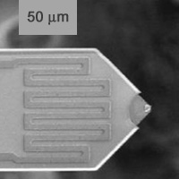
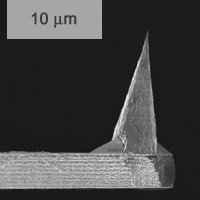
| SEM image of a self-sensing piezo-resistive cantilever with SCD tip. | Close view of SCD tip mounted on piezo-resistive cantilever. | |
AFM Lateral |
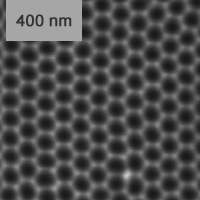
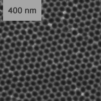
Scalloped Aluminium Gratings (SAG) are high precision hexagonal surface structures that can be used as AFM reference and calibration standards in XY plane. Unlike expensive submicron calibration gratings manufactured by lithography methods, SAG has repeatable and reproducible self-organized ordered structure with periodicity determined by the conditions of a simple electrochemical processing. The average periodicity within the domains is 102.5 nm (SAG-102) or 65 nm (SAG-65). Scalloped Aluminium Grating (SAG) can be used as an express method of AFM tip quality check. The hexagonal pattern of SAG consists of concaves and spikes, each concave is surrounded by six spikes. Because of the extremely sharp apexes of the spikes their experimentally observed radii on AFM scans exhibit the sharpness of the AFM tip. |
|||
 |
 |
|||
| SEM image of SAG-102 grating. Size 1x1 µm. | SEM image of SAG-65 grating. Size 1x1 µm. | Learn more >>> |
||