| Home | Probes | Applications | About us | Contacts |
|
|
Single |
SCD probe is a sharp micro-sized monocrystal diamond tip that provide highly reproducible results in AFM imaging, nanoindentation and lithography. The probe consists of two parts that are manufactured separately: a cantilever on a chip-holder and a tip. The tips grow in batches and then glued onto cantilevers using a specially developed micromanipulation technique. The manufacturing technology of diamond probes provides high product quality at reasonable costs. Images below illustrate key stages of the production.
|
|||||||||||||||||||||||||||
 |
 |
 |
 |
|||||||||||||||||||||||||
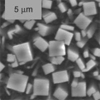
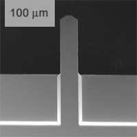
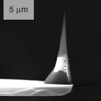
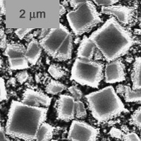
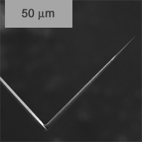
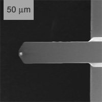
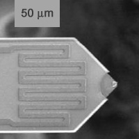
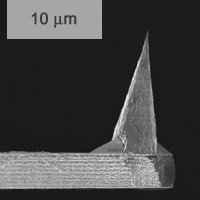
| Film of diamond crystals. SEM image. | Single crystal diamond tip of the needed size and shape separated from others. SEM image. | Tipless silicon cantilever. SEM image. | SCD tip mounted on silicon cantilever. SEM image. | |||||||||||||||||||||||||
Diamond Tips |
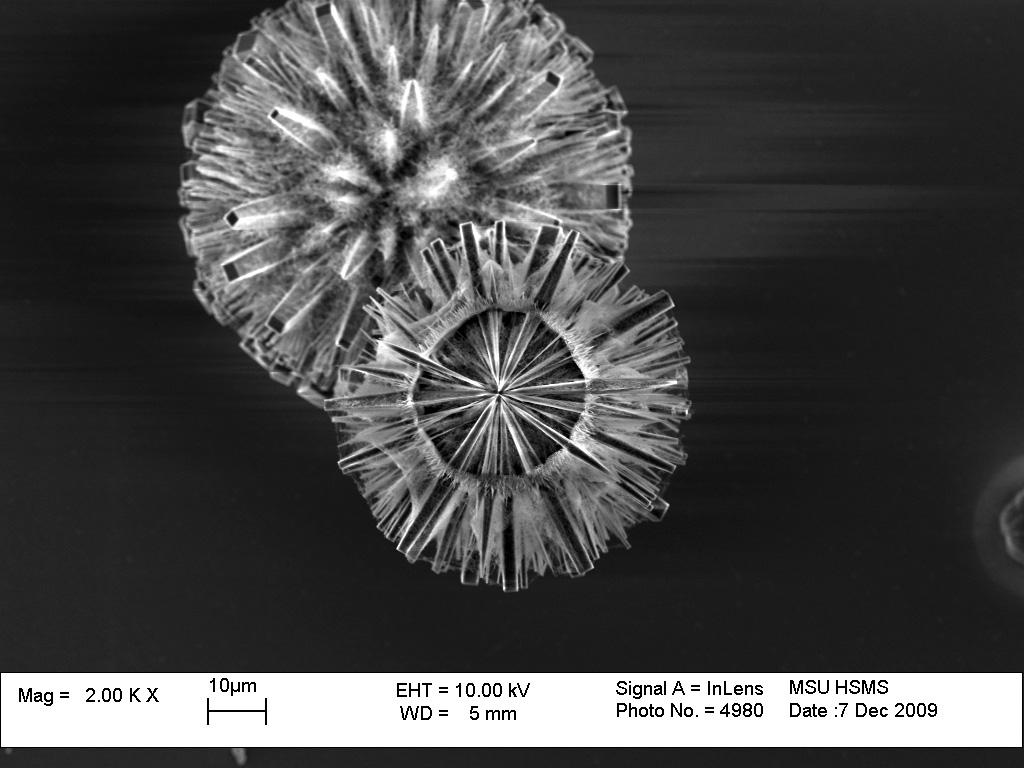
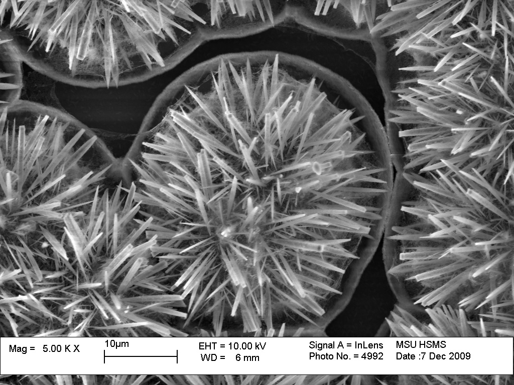
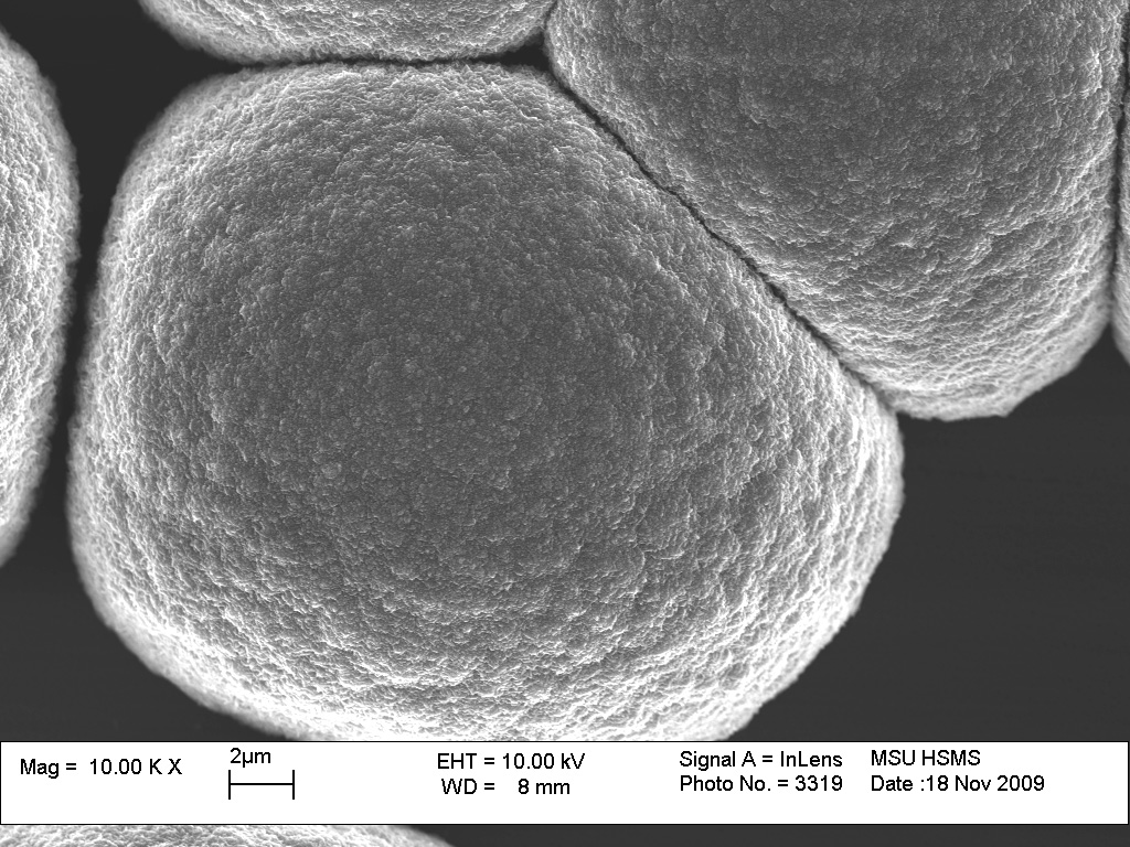
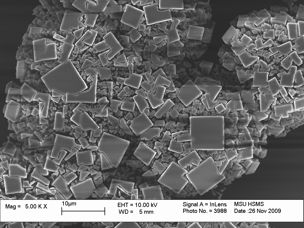
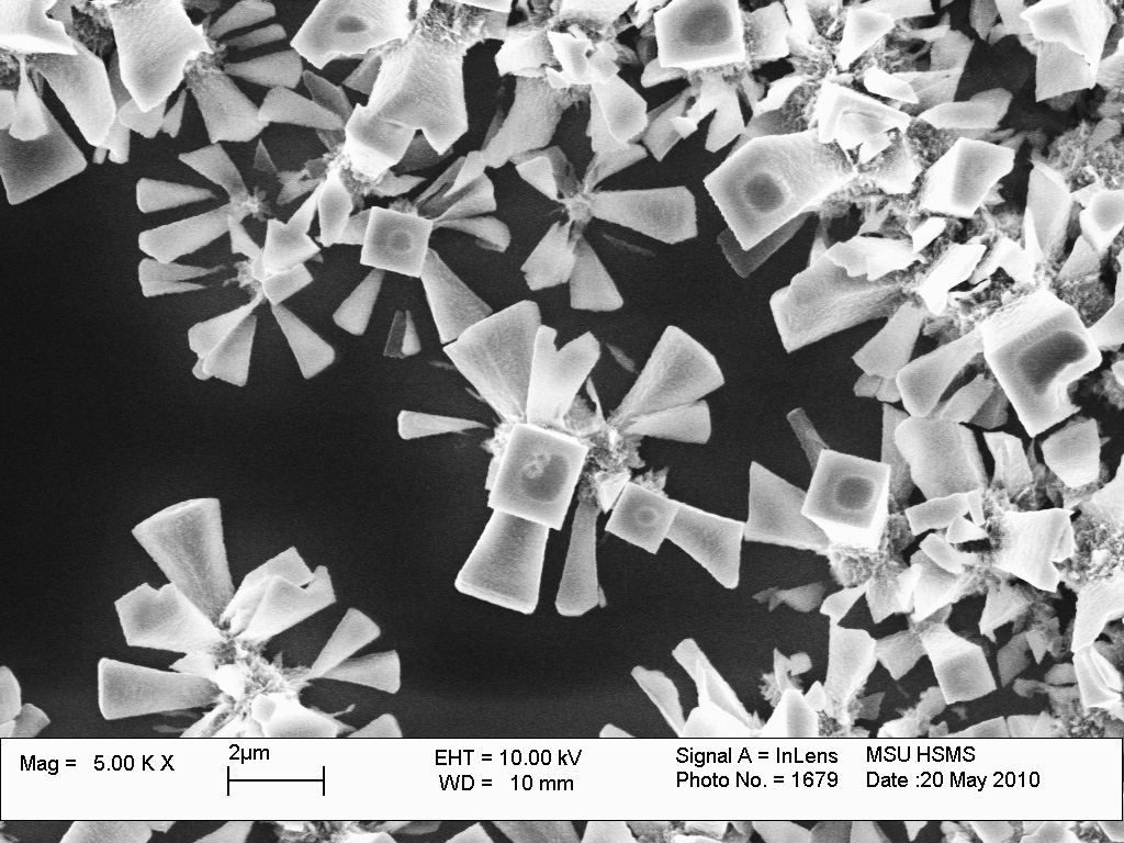
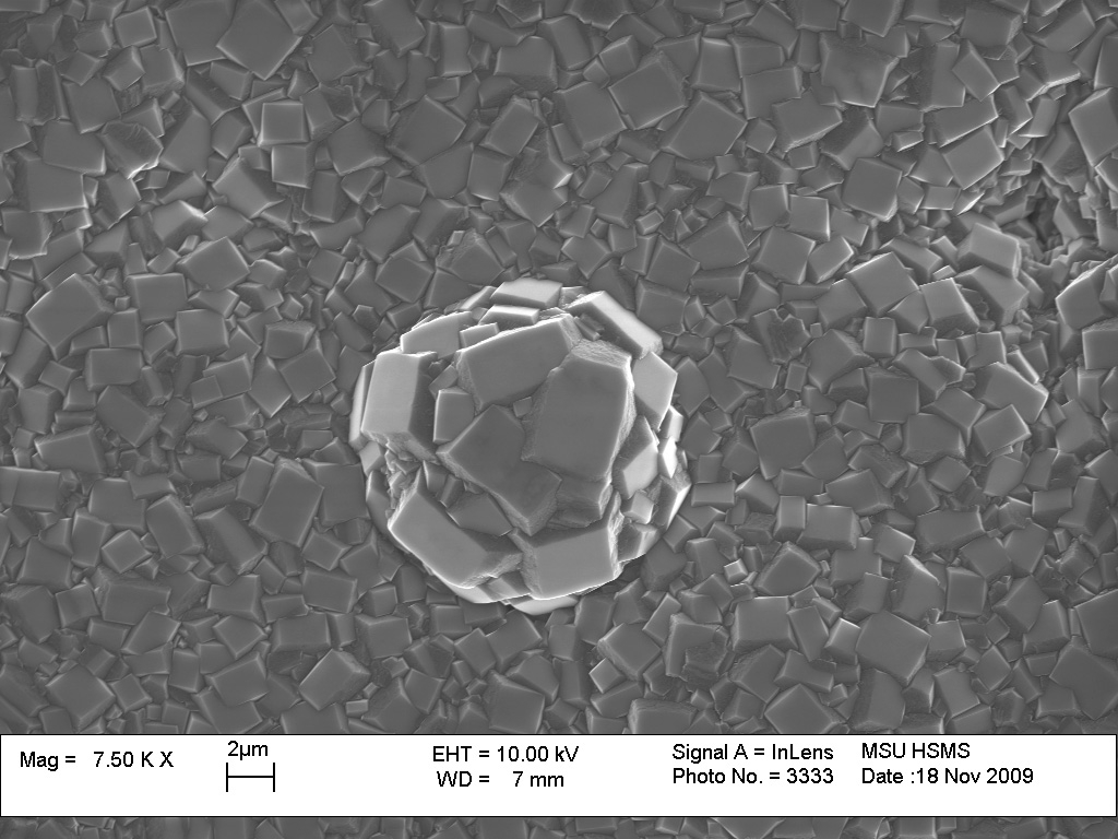
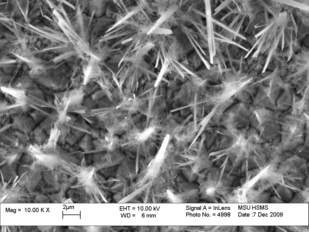
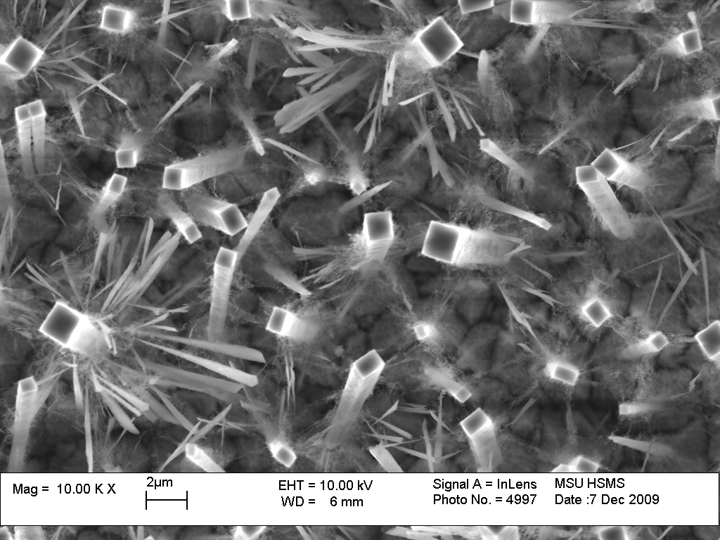
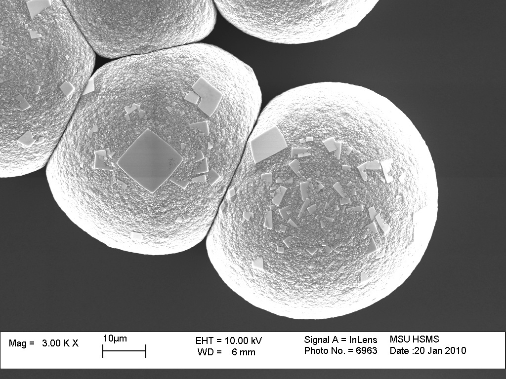
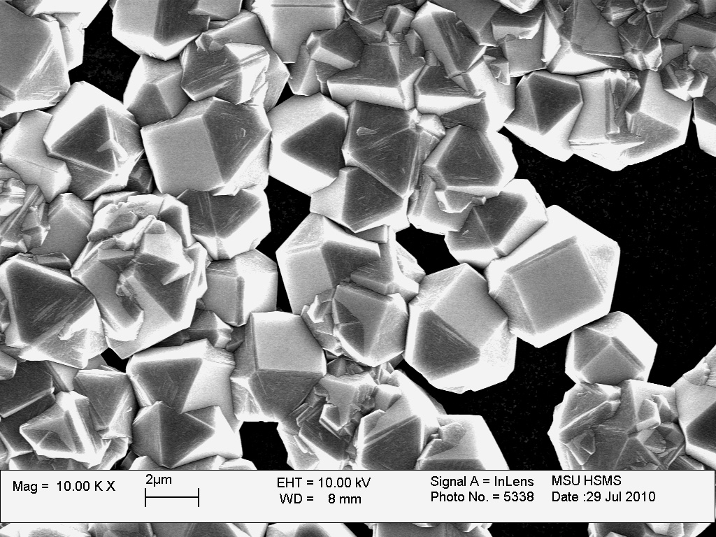
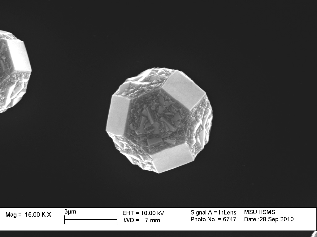
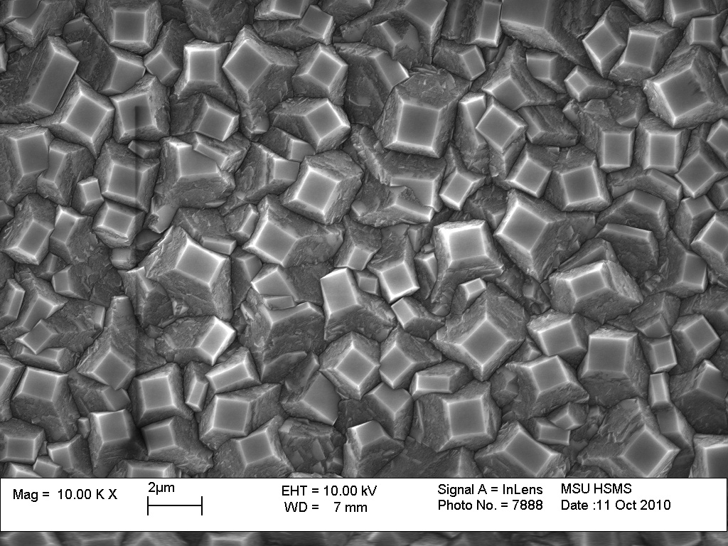
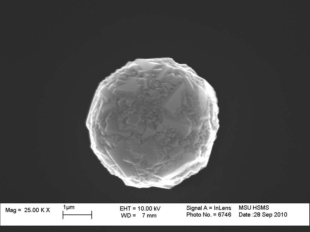
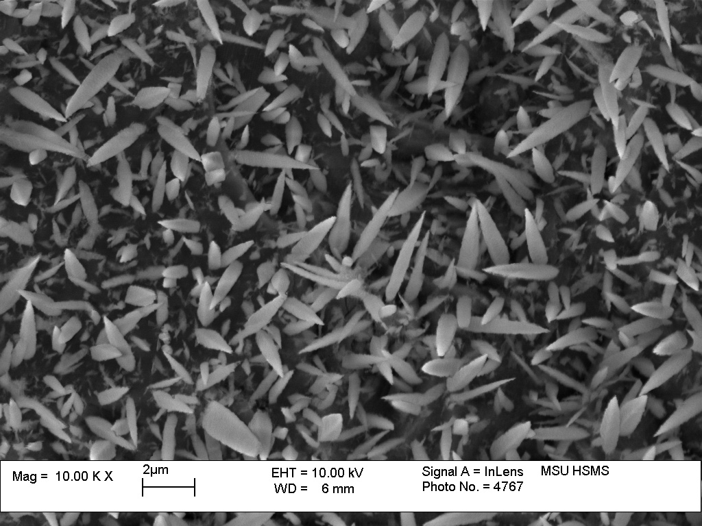
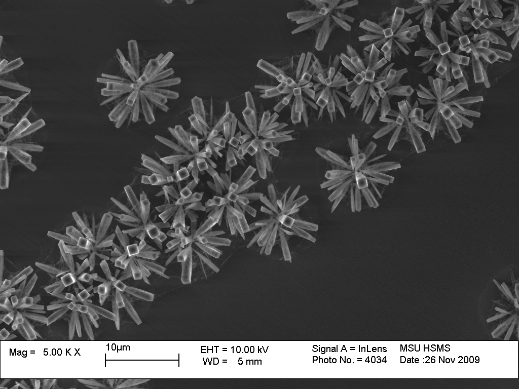
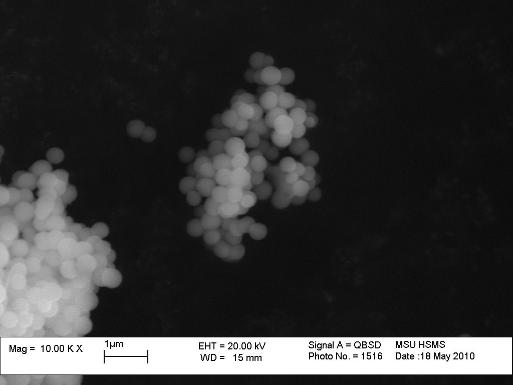
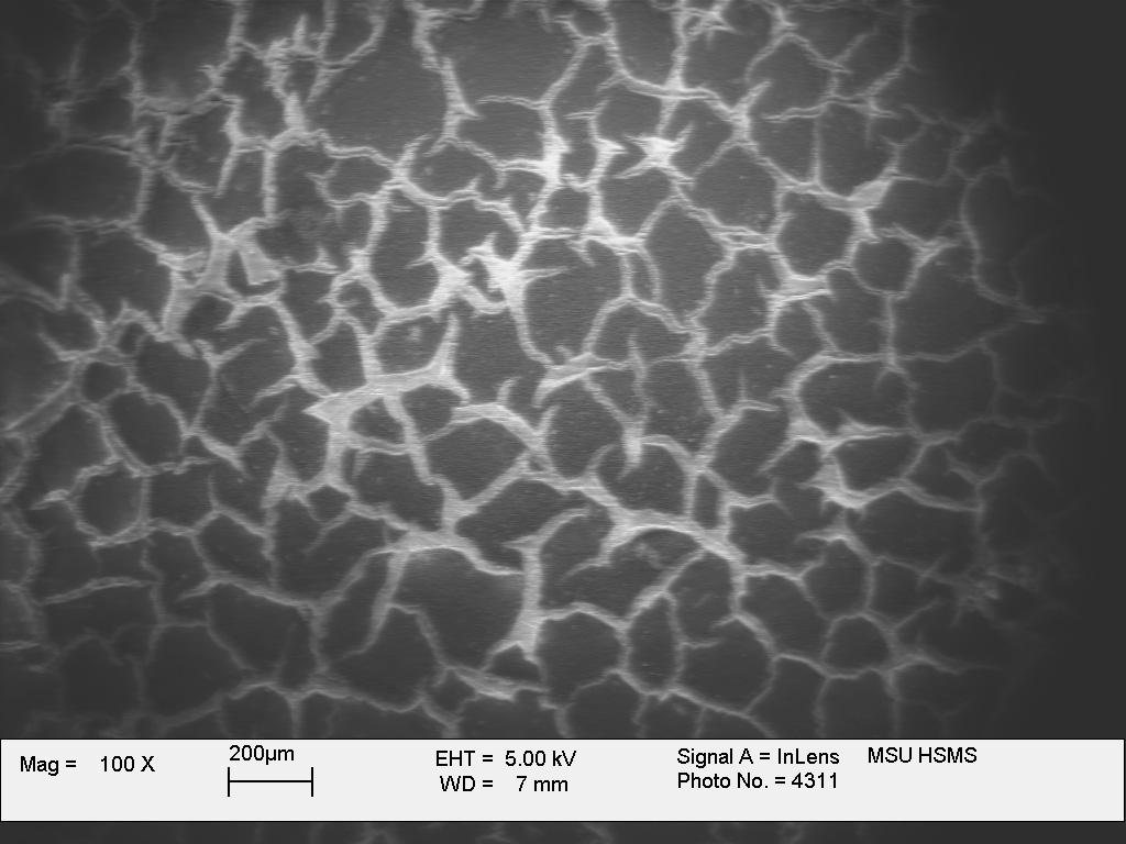
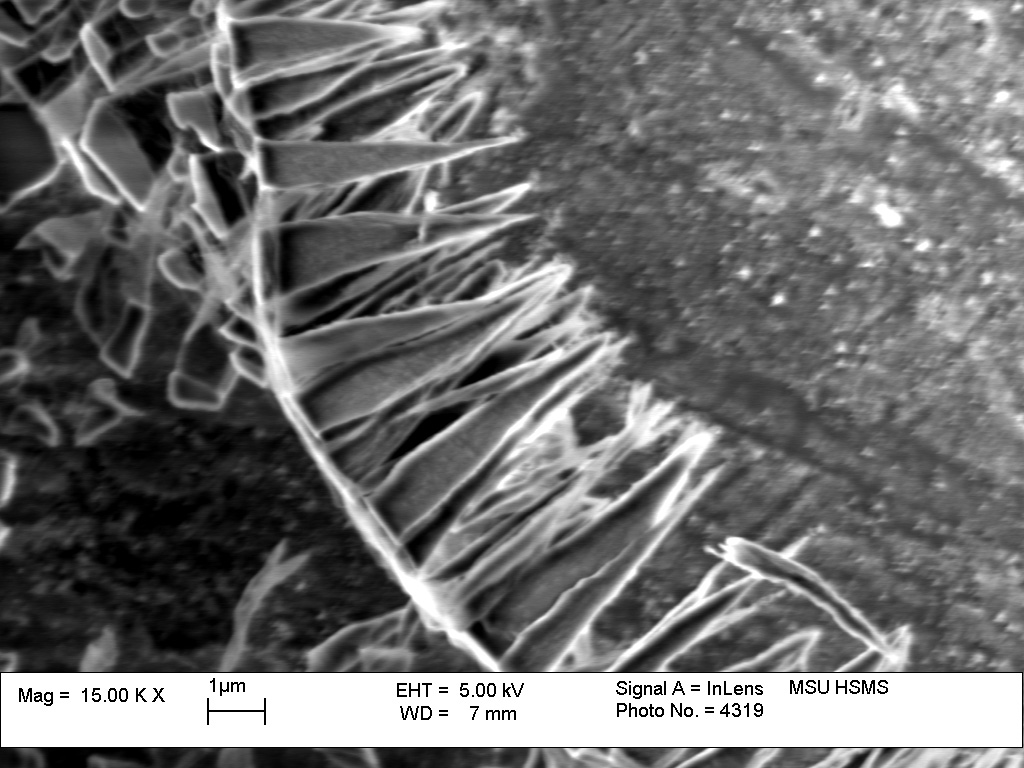
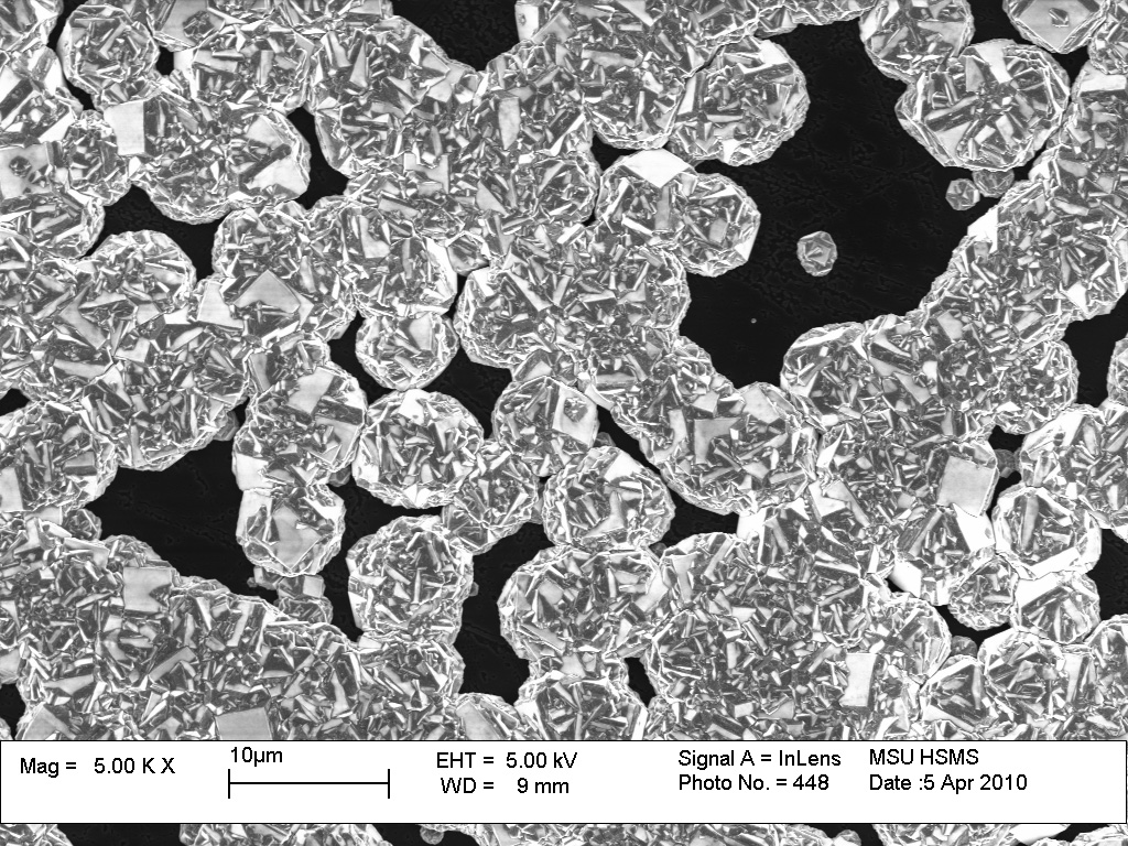
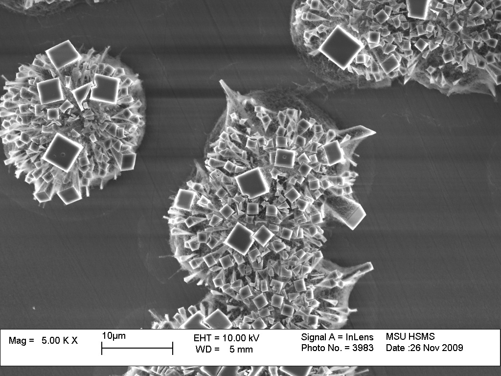
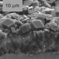
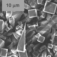
Still these techniques do not utilize the ability of a crystal to anisotropic growth, when it can get itself a shape specific for AFM probe tips. Such a diamond monocrystal must have higher hardness comparing to the polycrystals and better durability comparing to the films. This opportunity emerges when diamond crystals grow fast in the <100> direction; in this case the tip also obtains a square basis convennient for mounting it onto a cantilever. The fact that diamond crystals of this kind are possible to grow by CVD was established in the middle of 1990's [1]. The same technique under similar conditions allows getting fullerenes, graphenes and nanotubes, and the range of the technological parameters providing growth of each structure is quite narrow. Our know-how consists in the growth of monocrystal diamond pyramids with the {001} facet in the basis having a controllable shape along the <001> axis. What's challenging here in the view of AFM application perspective, it is to attain good sharpness and aspect ratio at the tip end. There are just some examples below on how the growth of the diamond pyramids may go. The growth usually starts from the formation of nanometer-sized nuclei with random orientations over the substrate. Along with the growth of the diamond crystals in the preferred direction, secondary nucleation starts on their lateral surfaces. All these crystallites form a ballas-like film contaning tips of the needed size and orientation and the "wadding" of satellites. Additional treatment is needed to remove the ballas-like diamond crystallites, while the large single crystal diamonds of pyramidal shape must remain untouched or just get "polished" in this process.
|
|||||||||||||||||||||||||||
|
|
|
|
|||||||||||||||||||||||||
|
|
||||||||||||||||||||||||||||
 |
 |
 |
||||||||||||||||||||||||||
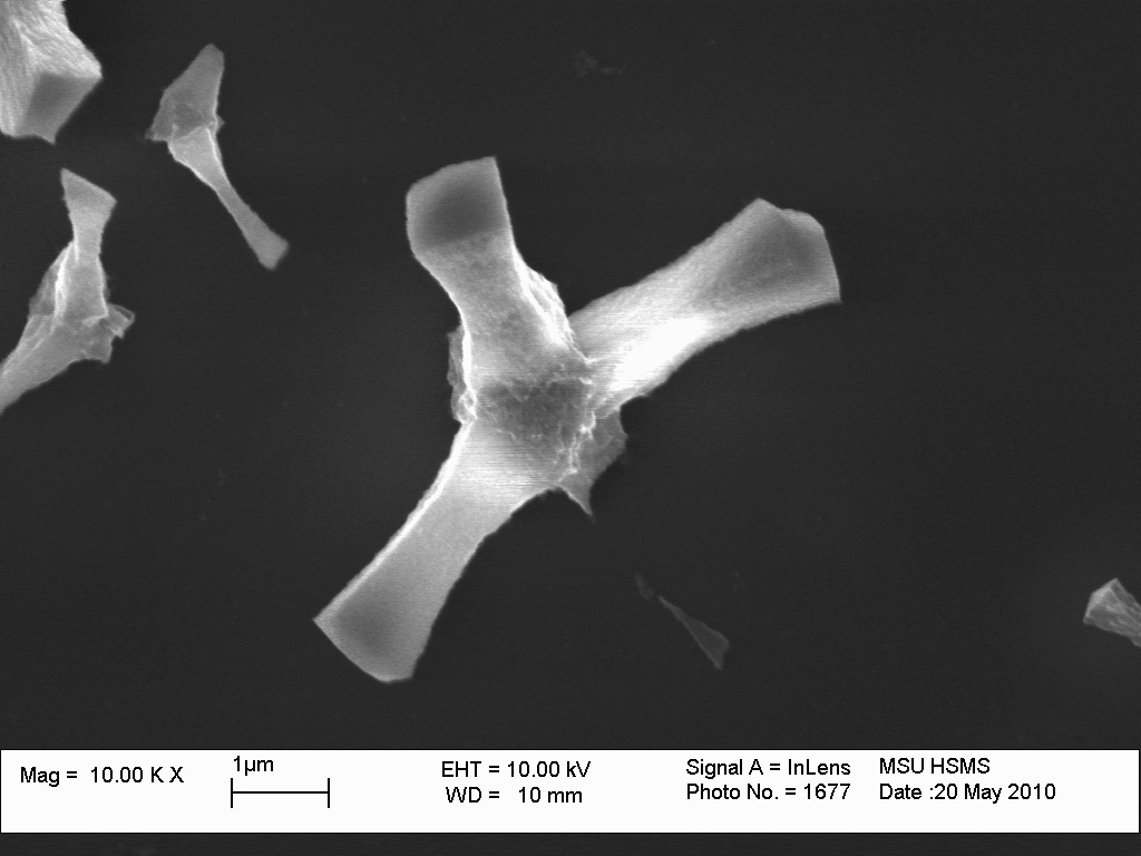
| Film of diamond crystals in the beginning of the growth. SEM image. | Cross-section of the ballas-like diamond film. SEM image. | Individual tip on surface of diamond film. SEM image. | ||||||||||||||||||||||||||
Micromanipulation |
|
|||||||||||||||||||||||||||
 |
 |
|||||||||||||||||||||||||||
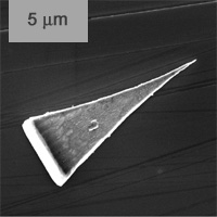
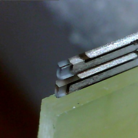
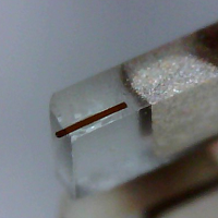
| Piece of etched carbon fiber glued to a silicon cantilever. SEM image. | Cantilever with attached diamond pyramid on the end. SEM image. | |||||||||||||||||||||||||||
|
|
||||||||||||||||||||||||||||
 |
 |
|||||||||||||||||||||||||||
| Photo of a cantilever attched to tuning fork for tapping mode AFM. | Close view of the same cantilever. | |||||||||||||||||||||||||||
|
|
||||||||||||||||||||||||||||
 |
 |
|||||||||||||||||||||||||||
| SEM image of a self-sensing piezo-resistive cantilever with SCD tip. | Close view of SCD tip mounted on piezo-resistive cantilever. | |||||||||||||||||||||||||||
Functionalization |
|
|||||||||||||||||||||||||||
|
|
||||||||||||||||||||||||||||
|
1. G. Knuyt et al. Diamond and Related Materials, 1998, v. 7, p. 1095. 2. (WO2009153116) DIAMOND NANO-TIP AND METHOD FOR PRODUCTION THEREOF. 3. A.N. Obraztsov et al. Single crystal diamond tips for scanning probe microscopy. Rev. Sci. Instrum. 81, 013703 (2010) 4. A. Majumdar, Ann. Rev. Material Science, 1999, v.29, p. 505 5. C. Manfredotti et al., Diamond and Related Materials, 1998, v. 7, p. 523. 6. R. Nelz, P. Fuchs, O. Opaluch, S. Sonusen, N. Savenko, V. Podgursky, E. Neu arXiv:1608.08369 | ||||||||||||||||||||||||||||